客服


单晶和多晶可选
颗粒结构
可选
是否有背胶
上海
公司地址
美国
原产地
张经理
主营: 研究和试验发展
上海市

The PlasmaEtch decapsulation system is a revolutionary patent-pending gas-based semiconductor etching system. Employing a never-before-seen application of microwaved gases inciting chemical radicals for isotropic etching, the PlasmaEtch is the greenest and most cost-effective etching solution available. The PlasmaEtch can etch most sample sizes, encapsulant types, and wire bond types. Whether it’s a more traditional gold wire sample, or if the sample features copper or silver wires, the PlasmaEtch delivers a safe and reliable etch.
PlasmaEtch创新点:
Afterburner Downstream Focused Plasma Etching(延时激发下行聚焦离子蚀刻)
Mass Flow Controlling for All Gases(所有气体流量可控)
No Microwave Radiation Exposure to Samples During Etch Process(无微波辐射)
Low Temperature Etching(低温蚀刻)
Isotropic Etching(等向性蚀刻)
Unlike typical and less sophisticated plasma decap systems that take many hours or even days to get to the surface of the die, the PlasmaEtch can clear the encapsulant of most package types and reveal the complete die surface and wire sweep in a matter of a couple hours. Chemical-free decapsulation has never been so effective.
主要特色(Highlights):
Highly Customizable Etch Recipes(高度可定制的蚀刻配方)
Etches a Wide Variety of Package Types(可蚀刻各种各样的封装类型)
Completely Chemical-free Decap(完全非化学方式蚀刻)
Eco-friendly(生态友好环保)
Touchscreen Interface(触控屏)
PC/Windows-based GUI(基于PC / Windows的GUI)
The Only Solution for Silver Wires(银线的解决方案)
Etches Samples with All Wire Types(可蚀刻所有引线类型的样品)
Small Footprint Suited for Tabletop(桌上型紧凑尺寸机柜)

OGP自动化高精度3D激光扫描仪-ShapeGrabber Ai810

OGP自动化高精度3D激光扫描仪-ShapeGrabber AI620

AXIS-TEC激光晶圆划片机AX-LS100

酵母显微操作仪 MSM400

HIRAYAMA高加速寿命试验箱PC-R9
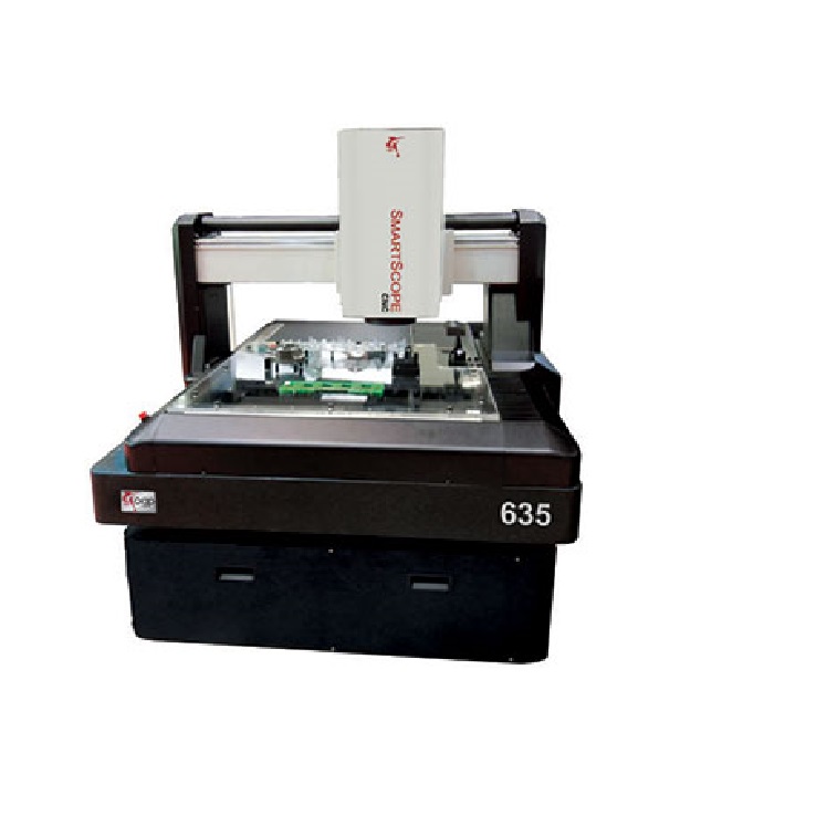
CNC影像测量 OGP测量仪
OGP自动化高精度3D激光扫描仪-ShapeGrabber Ai810
OGP自动化高精度3D激光扫描仪-ShapeGrabber AI620
AXIS-TEC激光晶圆划片机AX-LS100
酵母显微操作仪 MSM400
HIRAYAMA高加速寿命试验箱PC-R9
CNC影像测量 OGP测量仪
*采购数量: 件
采购数量不能为空
*联系信息:
联系信息不能为空
公司名称:
采购说明:
验证码不正确